Debugger for the 6502 and other CPUs
What is it?
The Debugger enables you to observe the behavior of the 6502, 6510, 6809 and Z80 processor step by step. I built it to debug some hardware problems I had with my Elektor computer, equiped with a 6502.The story
In 1986 I got an Elektor/Elektuur Junior for free but it was broken. For those who don't know the Junior, it is a 6502 based computer, quite the same as the KIM. It can be extended with lots of cards. I made some of the cards myself but they did not always work well right from the start. So I decided to build a device to check the status of the bus at a given moment: the Debugger.The idea
The idea itself is quite simple: stop the processor (CPU) and check the levels of all the lines you are interested in. But how are we going to stop the CPU? Most CPUs I know have an input to perform this job. For the 6502 this is the RDY input (RDY = ReaDY). Make it (L) and the processor stops. (Almost) as simple like that!The next thing is to determine the levels of all the lines you are interested in. The simplest way is to use some buffers and a lot of LEDs. But to make life easier I thought about using intelligent hexadecimal displays. Just connect the address and data lines to these displays and you have a nice hexadecimal output.
The last thing: were should I tap the signals? Instead of tapping the needed signals directly from the 6502 I decided to tap them from the provided bus.
(Almost) as simple like that!
My first 'almost' is a feature MOS/Rockwell implemented in their 65xx which I still don't understand: when the RDY input is negated during a write-cycle, the CPU does NOT stop! This meant that if something went wrong during that specific write cycle, I had no means to check it. Generally spoken this 'problem' caused no trouble because I could lay my hands on some 65SC02s from GTE and these CPUs have this nice feature that they do stop during a write-cycle as well :-)But then I decided to use the debugger for my C64 and C128 too by creating a card that could be placed in the expansion port. But as there is not such a thing as a "65SC10", I had to find another solution for the 'write-cycle-bug'. I only managed to solve it half. I 'froze' the data during this cycle on the displays by preventing an update of it immediately after a write-cycle. In this way I could see at least once what the CPU had written to where. But unfortunately there are occasions the 6510 performs two and even three write-cycles in a row (JSR, IRQ, NMI) and that means that some write-cycles still will be lost :-( Because of this and the fact that I hardly used this feature, I dropped it in this PCB version.
Another 'almost' was the accessibility of the RDY input of the 6510 in the C64 and the 8502 in the C128: in those days I thought that the DMA input performed this function. It does, but it also tri-stated the CPU. I found this out in the hard way. My first solution was to modify the board by placing an AND gate between the RDY input and the rest of the board using a new IC or using an unused AND gate on the board. For the new solution, see later.
The third 'almost' for the C64 is the VIC chip. As you probably know, this IC takes care of the videopart. This is done in such a way that the CPU and the VIC share the bus together but not simultaneously. Generally it means that the VIC controls the bus during the negative half of the clock and the CPU during the positive half. This mix of data meant that I only saw garbage on the displays of my original design. I solved this by reading the data only during the upper half of the clock and only when the CPU is not tri-stated.
Clicking and clicking and clicking.....
Using it with the Junior I soon discovered a serious shortcoming: it was not real usable for handling loops and subroutines. This meant you could be clicking that little knob for hours before you reached the address where the fault appeared. So I added an, what I called, address discriminator. This little device stops the processor at the chosen address.If the CPU does not stop, it means it didn't arrive at the chosen address which on its turn means that it started doing something else then you expected. The reason can be faulty hardware, an error in the software or you, misinterpreting the hardware and/or software :-).
The hardware
First two remarks:- The new hardware is not one single PCB but exists of two PCBs.
- The new hardware uses a GAL.
So this schematic:
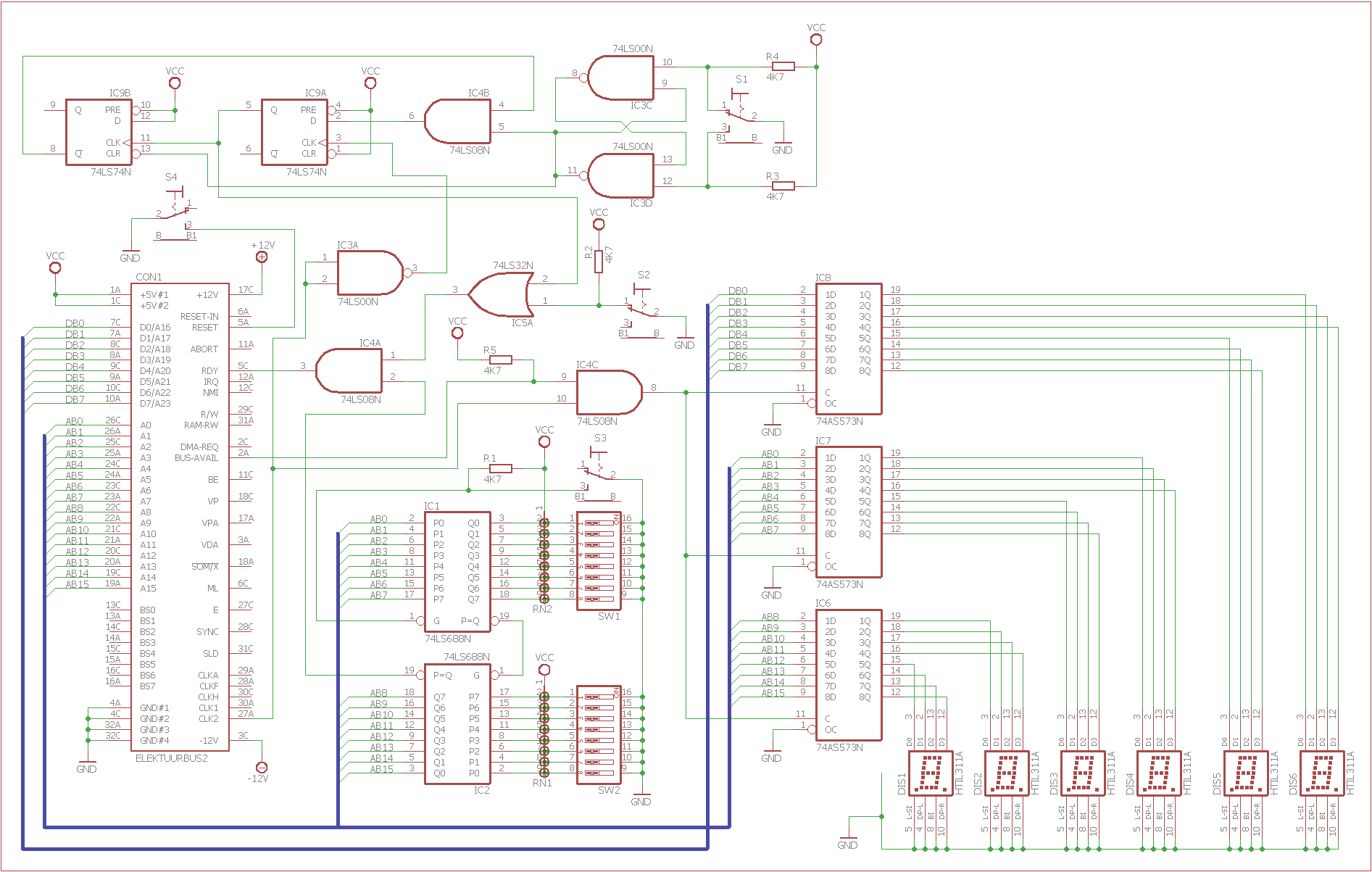
is not representing the actual hardware but is used to explain things. It can be divided in three parts:
- The logic to step the processor.
- The address discriminator.
- Enabling these circuits.
The logic to step the processor
First we have to debounce the switch that triggers the stepping. This is done by a flipflop, made out of IC3CB and D, two 74LS00 NAND gates. The output of IC3D is (L) when step switch S1 isn't pressed. This (L) is copied into output Q if IC9A, a 74LS74 D-flipflop at the rising edge of its CLK input = the falling edge of CLK2. This on its turn pulls RDY (L) and the CPU halts. Forget about IC4A, IC4B and IC5A for the moment.
             +----+    +----+    +----+    +----+    +----+    +----+    +----+
CLK2         |    |    |    |    |    |    |    |    |    |    |    |    |
        +----+    +----+    +----+    +----+    +----+    +/  /+    +----+

                   +---------------------------------------/  /--+
IC3D               |                                             |
        -----------+                                             +-------------

                    +----------+
IC4A                |          |
        ------------+          +---------------------------/  /----------------

                             +---------+
IC9a / RDY                   |         |
        ---------------------+         +-------------------/  /----------------
        ----------------------+                                   +------------
Q\_2B                         |                                   |
                              +----------------------------/  /---+
                   A         B C       D                          E

                                 Fig. 2
Now assume that at point A the switch is pressed and the output of IC3D becomes (H). Point A can be situated at any place between two negative edges of CLK2. At the first falling edge of CLK2, point B, the Q output of the flipflop IC9A, and thus RDY, becomes (H) as well and the CPU will start its next cycle. The rising edge of this signal causes IC9B to negate its Q\ output, point C. Now IC4A, an AND gate, will play its role. The (L) from this Q\ output is fed into IC4a and will cause to become its output (L) as well.
At the next negative edge of CLK2, point D, this (L) will be copied into IC9A's Q output, thus negating RDY and the CPU will halt again.
As long as switch S1 is pressed and therefore the output of IC3D remains (H), the Q\ output of IC9B will remain (L). The moment switch S1 is released, point E, the CLR input of IC9B is negated by the output of IC3D and its Q\ output becomes (H) again: the circuit is ready for th next step.
Just to be sure: with Q\ I mean the inverted Q output.
If you look good, you will see that there is a difference of one character between the falling and rising edges of the various signals. This difference represents the delay times of each gates. They are only about 10 ns but even this can be enough to have a significant meaning in certain situations. Certainly in case of clearing D-flipflop IC9B. These few nanoseconds make sure that pin 5 of the and gate IC4B is (L) before pin 4 becomes (H) and no glitch is generated.
We must be able to enable or disable the stepping circuitry. If we connect the Q output of IC4B directly to the RDY input of the 6502, the 6502 can never run at full speed. The simplest solution is to place an OR gate, IC5A (74LS32), in this line. The second input of this gate is connected to switch SW4 and a pull-up resistor. Opening SW4 means that the OR gate, and thus RDY as well, becomes (H) which means the 6502 can run at full speed.
Afterthought: what about placing switch S2 in place of the OR gate?
The address discriminator
The address discriminator is made out of two 74LS688's, IC1 and IC2. The 688 is an 8-bit comparator. One side is connected to the address bus, the other side to an 8-bit dipswitch plus pull-up resistor-array. The idea is simple: the moment both 8-bit sides see the same input, pin 19 becomes (L). IC1 cascades its output to IC3A, a 74LS08 AND gate. The function of this gate is to mix the signal from the discriminator with the one coming from the stepping circuit.
A pull-up resistor and switch SW3 connected to pin 1 of IC1 enable or disable the discriminator.
A reset switch
As an extra I added a reset switch: S4.
The schematic will probably have one small mistery for you: why did I use NAND gate IC3A on the main card to invert CLK2 and why didn't I use CLK1? The reason is quite simple: CPUs like the 6510 and 8502 don't generate CLK1. And this simply means I have to generate it myself..
How to operate the debugger.
Opening switch S2 disables the step-circuit. Opening switch S2 disables the address discriminator. One starts with setting the address where the CPU should halt, closes switch S3 and resets (switch S4) or powers up the computer. The system shoukld halt at the given address now. We now close switch S2, thus enabling the step-circuit which will halt the CPU at this moment as well. Now we open switch S3, thus disabling the address discriminator. Now we can start stepping.The real hardware, GAL version
This desin of a PCB looks more or less like the original one: LED displays and switches were placed on the PCB. But there is a difference was: one of my Elektor computers is built in a 19 inch rack which meant that the dip switches were hardly accessible. And why using dip switches, why not thumb wheels with hexadecimal output?So I replaced the two dip switches with two 10-pin connectors and combined the 6-pin and 4-pin headers to another 10-pin one. This enables me to connect this PCB with another one that contains the various switches.

The GAL only replaces the logic gates, not the two D-fliflops. The reason: I have no idea how to program a D-fliflop in a GAL. Of course I asked around and the only soulution I got meant that I could create one but only one. But as I need two D-flipflops, I still needed an extra IC.
Have a look at the PCB:


The GAL
GAL IC1
	Name		-- Debugger Elektuur GAL--;
	Device		G16V8;
	Designer	Ruud Baltissen;
	Date		2023-11-14;
	Revision	V0.1;

	Assembly	--;
	Company 	--;
	Location	--;
	Partno 		--;


/* Define Logic Operators */
	/* AND = &  */
	/* OR  = #  */
	/* NOT = !  */
	/* XOR = $  */


/* Define Input Pins */
pin  2 = JP3_5;		/* switch S1, pin 1 */
pin  3 = JP3_1; 	/* switch S1, pin 3 */
pin  4 = JP2_1;		/* switch S2, pin 1 */
pin  5 = LS688;		/* output of 2nd 74LS688 */
pin  6 = BA; 		/* Bus Available, pin 2A of the bus */
pin  7 = CLK2; 		/* pin 27A of the bus */
pin 13 = IC9BNQ;	/* output /Q of IC9A */
pin 14 = IC9AQ;		/* output Q of IC9B */

/* Define Output Pins */
pin 15 = TMP;		/* output of IC3A */
pin 12 = RDY;		/* pin 5C of the bus */
pin 16 = IC9BCLR;	/* input CLR of IC9B */
pin 17 = IC9ACLK;	/* input CLK of IC9A */
pin 18 = IC9AD;		/* input DATA of IC9A */
pin 19 = S573CLK;	/* input CLK of the 74ALS573s */

/* Boolean Equations */
TMP	= !(IC9BCLR & JP3_5);
IC9BCLR	= !(TMP & JP3_1);
IC9AD	= IC9BNQ & IC9BCLR;
RDY	= (IC9AQ # JP2_1) & LS688;
IC9ACLK	= !CLK2;
S573CLK	= CLK2 & BA;
Connecting the card to a non-Elektor computer
This card will, as it is, only work in a computer with the Elektor bus, like the Junior, EC65 or a DOS65 machine. So what about other computers? The solution is simple: I designed little PCBs that has to be placed between the original CPU and the motherboard.For the 6502


For the 6510


For the 6809


For the Z80


The schematics and boards all look almost the same. What will stand out are the two AND gates and the two or three jumpers. Why the jumpers? I once ran into a situation where IRQs disturbed the test. Lifting the IRQ pin out of its socket solved the problem then but it is not ideal. So the jumpers enable you to disable the various interrupts: IRQ, NMI plus FIRQ in case of the 6809.
The reset and RDY line of the Elektor bus are both open collector lines. I cannot expect that to be the case for any other 6502 system and those AND gates solve that problem: they mix the original signals with the ones generated by the card.
The successor if this card, Debugger-LPT, gave me the possibility to monitor some extra lines: R/W, NMI and IRQ in this case. So even if due to missing jumpers IRQ and/or NMI arn't serviced, you can still see if one has been generated by the system.
Other processors.
I already mentioned the fact that the original idea, a card that you stuck into the expansion port did not work out. In these cases I decided to use the same solution as above: PCB that have to be placed between the original CPU and the motherboard. So far only the PCB for the 6510 is available.The schematic will probably solve a small mistery: why did I use NAND gate IC3A on the main card to invert CLK2 and why didn't I use CLK1? The reason is quite simple: both the 6510 and 8502 don't generate CLK1. Solving the problem on the main card meant that I needed less hardware on the sub boards.
The switches
The original version had the switches on the board and, as explained above, I had reasons to make a separate board and connect them with flatcables. I created a separate page for it: Debugger Switch Board.Debugger-LPT
I already mentioned this card above and it sounded if that that successor is better than this one. But I found out that I had to change my mind about that. Main reason: with the Debugger-LPT I need a second computer to see the results and the original Debugger I can use stand-alone.You can email me here.