Build your own Memory Management Unit
What is it
Read the page about the 74LS612 MMU first to find out what a MMU, Memory Management Unit, is and does. This schematic enables you to build your own MMU.
The story
After designing the PC-Card (discarded project) I decided to make a version for 6502 based computers. This design enabled the user to expand his computer to 16 MB using a 65816, a 74LS612 MMU or both. Unfortunately I found out that both ICs are hardly available. So I decided to design a MMU using normal available ICs.The design
The core of the 74LS612 is made of sixteen 12-bit wide registers. The idea rose to use two 20 ns 2K*8 cache SRAMs. The delay of 20 ns is not critical as the buildup of the address is somewhere halfway the lower half of PHI2.Having 16 bits to our proposal means we can do more with this design then with the 74LS612. Using four more address lines means we could expand a system up to 256 MB! On the other hand it gives us the opportunity to reduce the size of the individual pages. Using the 74LS612 the size of a page is 4 KB. My idea is to add two other lines to reduce them to 1 KB.
Why 1 KB? The total I/O area of the PC is just 1 KB big. The video RAM of the CBM/PET is just 1 KB. The text-only video RAM of the PC, 2KB, and I/O area could fit neatly in the $8xxx-area not used by the CBM/PET.
Next thing to cover is the output of our MMU. The output is either the original lines or the programmed ones. 257A's are used to switch between them. When in "Original mode", A16..23 become (L). The 257A enables you to tristate the MMU if needed.
The input side uses the same idea: in "Original mode" the address line A0..A5 are connected to the SRAMs, in "MMU-mode" the address lines A10..15 are.
The control lines OE and CS are tied together. In "Original mode" they are activated when the MMU is selected. In "MMU-mode" they are activated all the time.
The WE input is hold (H) during the "MMU-mode" ensuring the SRAMs output their contents all the time. In "Original mode" they are connected with the CPU's R/W line.
How to handle 16 input lines.
The chance is quit big you will use this MMU with an 8-bit CPU. The 12-bit wide data bus of the 74LS612 already proved to be a problem. Andre Fachat's GECKO only uses 8 bits but the penalty is he only can address up to 1 MB.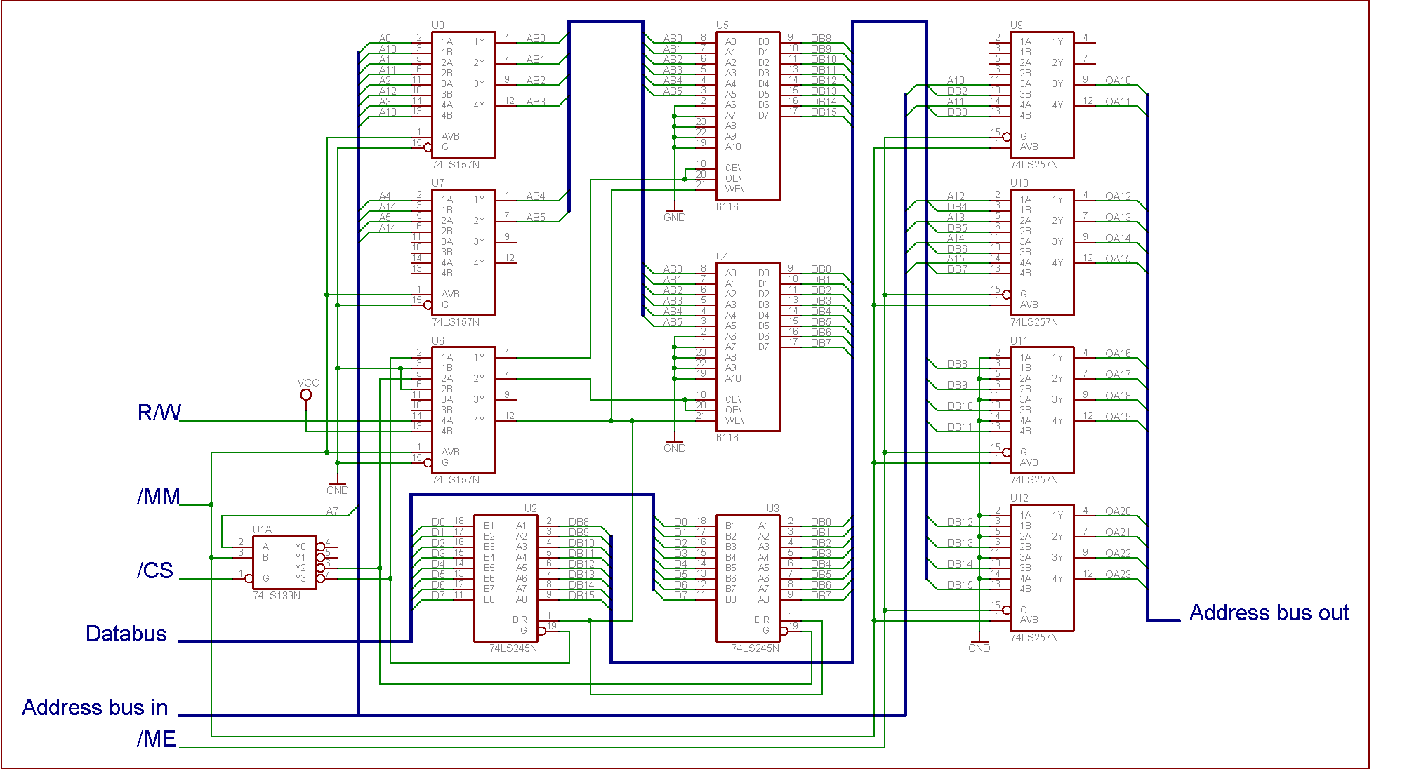
I got rid of this problem by using an extra address line and a 139 demultiplexer to be able to handle each SRAM separately through a 245 buffer. The 139 also provided a neat way to disable these buffers when in "MMU-mode".
Schematics
This MMU has the same connections as the already mentioned 74LS612 MMU. But how does it work?When the MMU is not active, ie. the input /MM is (H), two 74LS157 multiplexers, U7..8, feed the RAMs with the address lines A0..5. A third 74LS157, U6, takes care of providing the RAMs with the correct enable and read/write signals. Together these three 74LS157s enable the user to change their contents.
On the other side the two 74LS257 multiplexers, U9..10, output the original address lines. Two other 74LS257s, representing A16..23, output only (L)s.
When the MMU is active, the RAMs are provided with the address lines A10..A15 and U9..12 output the new address lines A10..23.
Because the RAMs have to output their data at the same time in this mode, they must have separate data busses. That's why we need two 74LS245 bidirectional buffers to change/read their contents. U1A takes care of this selection.
Expanding the design
Multiple configurations.Only needing 6 of the 11 address lines of the 2K RAMs means that the rest has to be tied to GND. Or..... Connecting these lines to a latch means we can store multiple configurations. Instead of giving up to 128 commands to change from one configuration to another, just one will do. OK, the configurations have to be stored in the MMU first but that is the only time you need to apply so many MMU commands in row. For the rest it is just one command. (Unless you change a complete configuration of course)
We need a latch for the /MM input anyway. If we can combine it with this configuration latch, no address is wasted.
The MMU starts to occupy too much space....
Using a 16 bits wide MMU with 7 address lines means it will occupy 128 bytes memory. Adding the latch mentioned her above means it will occupy 256 byte. So my next idea is using a latch for the other address lines as well. The advantage is that the MMU will only occupy four bytes: two latches and the MMU data.We can use 74ALS374s or 574s if we want to read the contents of two 273's, we need two 541's. This totals 80 pins. Being very lazy I dreamed up another idea.
Using a 6522 or 6526 means we only have to solder 40 pins. If we use CA2 or CB2 to activate the MMU, saving an external register in this way, we'll need 16 bytes.
Andre Fachat's 74LS610 MMU
Andre Fachat made a replacement for the 74LS610 MMU.You can email me here.