The VIC-20 expanded
What is it
Maybe you are familiar with this project: expand your VIC-20 with some extra memory. This does the same, plus quite some extras.The idea
Cleaning up the room I ran into the board used for this memory expansion project, the onboard version in this case. The idea rose to make better use of it. One idea was equiping it with a 65816 CPU, version 1 of the 6502 -> 65816 project. A second idea was fitting it with RAM under ROM, like in the C64, so I could test new ROMs. Third idea: a big FlashRAM that contains multiple ROMs. And last but not least: an old dream, an ISA expansion bus. But I will describe those ideas in a separate page.The design - an extra 6522
Using RAM under ROM means we also need a circuit to control it. The C64 uses the onboard port of the 6510 for this purpose. Why not adding a 6522? Being lazy I decide to piggyback it on an existing one. And where to place it in the memory map? The orignal ones are found at $9110 and $9120. The "weird" addresses are caused by the fact that both ICs have a common chip select line, representing $91xx, connected to CS2 but A4 connected to CS1 of one 6522 and A5 connected to CS1 of the second 6522. In this way one could program both ICs at the same time by sending data to address $913x. OTOH, reading from $913x would cause a bus collision!The above means that $9100 is free to use for our pupose. A NOR gate connecting A4 and A5 to the CS1 input of the third 6522 could do the trick. "Could", see later.
The design - extra RAM memory
To place the 62256 32 KB RAM ICs, I removed the BASIC ROM and soldered it on top of the system ROM. The last one was socketed so in case of troubles or replacement both could be removed quite easily. Just the chip select line to the BASIC ROM has to be (de)soldered.I soldered a 24-to-28 pins converter on the spot of the former BASIC ROM and placed two piggybacked 32 KB SRAMs in it. The CS and OE inputs of the first one were connected to a combination of 3 input AND gates that combined the RAM1..3 and BLK2..4 onboard signals. After connecting the CS and OE inputs of the second SRAM to +5V the whole could be tested by powering on the VIC-20. The screen should show now 28159 free bytes.
Creating the RAM-under-ROM proofed not to be that easy. The problem was the needed amount of ICs. That's why I decided to use GALs for a change. And it paid off! To make a long story short: to realize the whole plus some extras, I only needed one GAL20V8.
For various reasons I decided to make it only possible to replace BLK5, the BASIC ROM and the System ROM with RAM.
The design - FlashRAM
One idea was to replace the orignal ROMs with a FlashRAM. But the GAL enabled me to have both. The GAL also enabled me to make the FlashRAM writable or not. And now the advantage of having both: if writing the FlashRAM in-system goes wrong, I always have a fall-back: the original ROMs.Normally only the System ROM is replaced by another one. But I decided to replace both with one FlashRAM. Using a 29F010 I still can have eight complete replacements!
The first idea was using switches or jumpers to select the needed combination. Then I got a bright idea: why not using the the 6522 here as well? After a hard reset a menu enables you to select the needed combination. And if you are in a hurry, you can still use the switches/jumpers. The original combination for example, is not aware of the third 6522 and won't initialize it. So the ports remain in input mode and the jumpers cannot harm the output buffers.
The design - the LPT interface
Having a new 6522 and only using 6 lines (so far), means I have 14 left for other purposes. So the idea rose to use the rest for an interface with the LPT port of a PC that can be used to load/save data/programs from/to the PC.The design - the GAL
I piggybacked the GAL on top of the two ROMs and then I soldered all the needed wires. And they are not soldered according the schematic! If I had adjusted the schematic to the reality or soldered the wires according the schematic, one of them would have looked like a mess. Using the schematic as a general lead, the PLD file will tell you exactly how I soldered the wires.The above show you another advantage of GALs: you can use input and outputs in the order you like, just adjust the source files!
For more info on PLD files: What are PLD files?
Building it....
The result: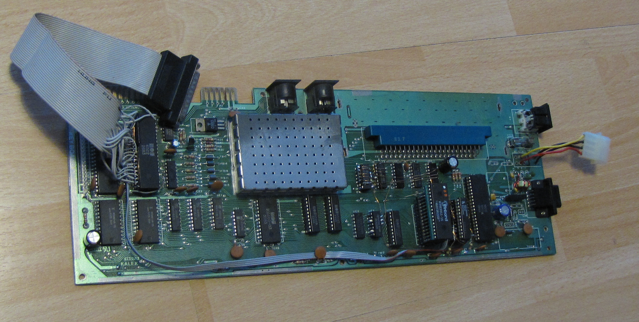
More Pictures:


You can email me here.